
The conductive material surface treatment
Thumbnail
-
Information
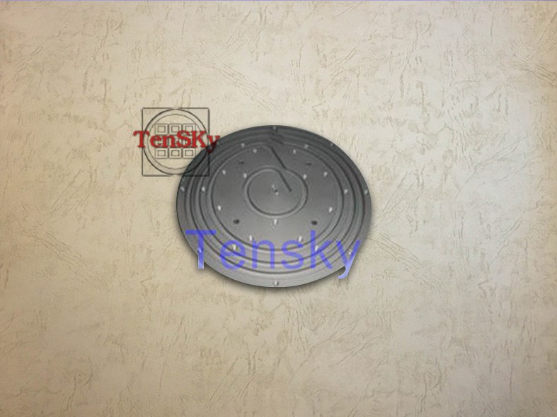
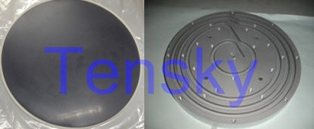
Should the market demand, the company has developed a conductive material, a conductive and anti-plasma and other characteristics, can be applied to photovoltaic and semiconductor industries, such as broken the back of the nickel plate to replace the application layer to improve the ease of re-use of time and offensive production.
-
Q&A
